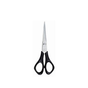
Fiskars Ciseaux loisirs creatifs ''ReNew'' ambidextre 13cm. Lames recyclees
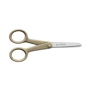
CISEAUX MATERIAUX RECYCLES RE NEWLes lames en acier inoxydable durables et recyclees (85 95 %) sont de precision rectifiee pour une nettete longue duree.Les poignees ergonomiques faites de plastique et de la cellulose renouvelable Emballage 100% recycles (fibres de papier recycles) et recyclables.13 CM bouts rondsProduit eco responsable :Recycle a 100%Recyclable a Offre exclusivement reservee aux professionnels