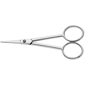
Westcott Ciseaux a silhouette, en metal, pointu, L : 100 mm Lot de 2
Lames en acier inoxydable, pour droitiers, des decoupesdelicates Offre exclusivement reservee aux professionnels
Lames en acier inoxydable, pour droitiers, des decoupesdelicates Offre exclusivement reservee aux professionnels
Cette paire de ciseaux est specialement concue pour des ongles forts avec de toutes petites lames et branches tres longues demultipliant la force une coupe aisee d'orteil.
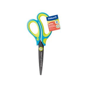
Avec zone de prehension douce pour une utilisation facile,avec plaque d'identification, smiley griffix aider atenir les ciseaux correctement, lames pointues, longueur:150 mm, droitiers Offre exclusivement reservee professionnels
La gamme Candy : elle est pop, acidulee et coloree comme des bonbons ! Ciseaux Wonday bicolores et bi matiere. Lames 17 cm en acier inoxydable avec large biseaux.Bouts pointus.Anneaux asymetriques bi pour plus de confort.Deux coloris disponibles : blanc rouge , bleu. Offre exclusivement reservee professionnels
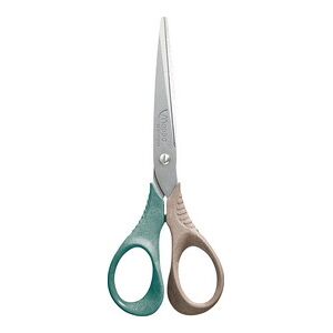
Smiling planeteAnneaux fabriquees a base de 50 % de fibre de bois certifiee FSC 100 % issu de forets gerees de facon responsable.Ergonomie 3D pour une meilleure tenue.16 cm DroitierProduit eco :FSC Offre exclusivement reservee professionnels
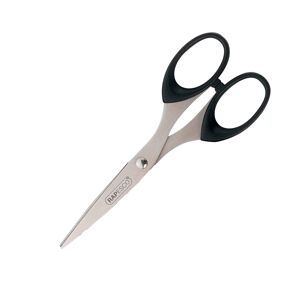
Ces ciseaux Rapesco vont aussi bien droitiers qu'aux gauchers. Lames en acier inoxydables, deux fois trempees.Poignees lisses en ABS. Dimensions lames : 160 mm.Garantis de 3 ans. Offre exclusivement reservee professionnels
Des ciseaux ambidextres ideals pour l'apprentissage. Ciseaux bout rond.Anneaux symetriques en polypropylene.Lames en acier inox trempe, 10 cm.Coloris bleu fonce. Offre exclusivement reservee professionnels
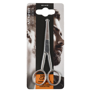
Menhir Ciseaux Poils Nez Inox vous debarrasse de vos poils de nez sans blesser grace a son bout rond. Cette paire de ciseaux a permet de couper en toute securite et offre une finition impeccable.
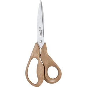
Ciseaux Advanced WoodDes ciseaux encore plus green !Anneaux ergonomique constitues a 50 % de fibres de bois.Lames et rivet en acier inoxydable.Confort et precision pour chaque type de prehension ou taille de main.Sous blister.Longueur 21 cm Offre exclusivement reservee professionnels
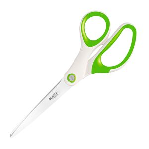
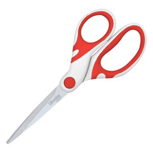
Une paire de ciseaux robuste et ergonomique pour toutes vos decoupes ! de design et innovante qui conviendra parfaitement a tous !Lames en acier inoxydable allemand de grande qualite. Le revetement titane confere une plus resistance lames. Ultra acerees, ces vous procure efficacite et longevite. Poignees bicolores et ergonomiques prise en main.Lames longueur 21 cm.Couleurs : rose, turquoise, menthe, orange, violet, vert pomme. Offre exclusivement